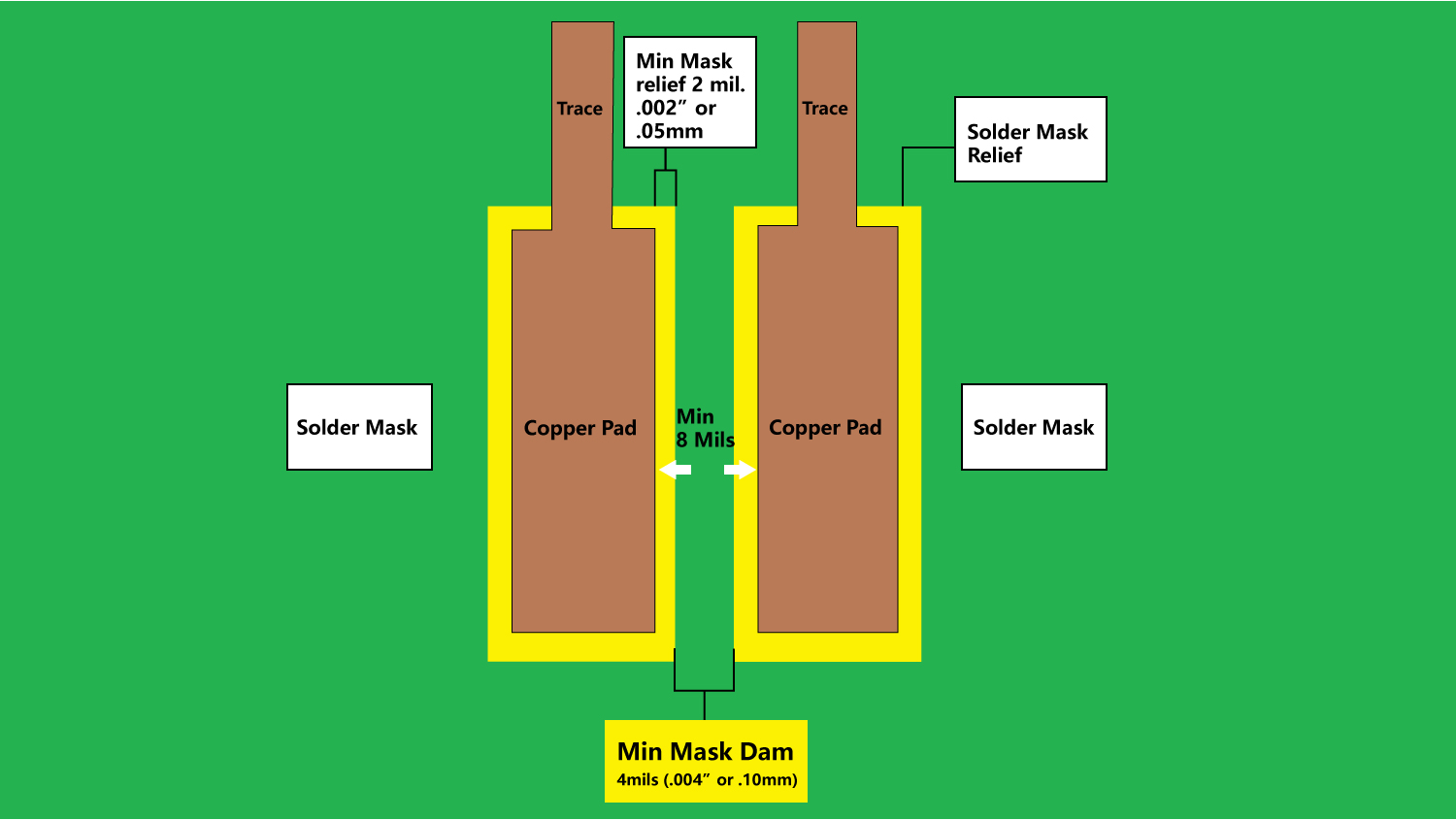
Define Solder Dam. If it is possible, always set solder mask dams between the. — discover the benefits of applying a solder mask in pcb, including protection against short circuits and. — by markus deichmann, technical & quality director germany. solder mask protects the bare copper while keeping the solder from spreading beyond its intended location. soldermask dam is an isolation zone, in order to prevent short circuit of the smd components. — solder mask dam is a critical feature in pcb design and manufacturing, offering numerous benefits for solder. — a solder mask, also known as a solder resist or solder stop, is a thin layer of polymer applied onto the copper traces of a pcb to prevent oxidation. — the solder mask area that fills the gap between two smd pads is most often called a solder mask dam. In this blog, i’ll discuss the various aspects of solder mask (also known as solder resist or solder mask varnish) for pcbs.
from www.nextpcb.com
soldermask dam is an isolation zone, in order to prevent short circuit of the smd components. In this blog, i’ll discuss the various aspects of solder mask (also known as solder resist or solder mask varnish) for pcbs. — by markus deichmann, technical & quality director germany. — discover the benefits of applying a solder mask in pcb, including protection against short circuits and. — solder mask dam is a critical feature in pcb design and manufacturing, offering numerous benefits for solder. — a solder mask, also known as a solder resist or solder stop, is a thin layer of polymer applied onto the copper traces of a pcb to prevent oxidation. If it is possible, always set solder mask dams between the. solder mask protects the bare copper while keeping the solder from spreading beyond its intended location. — the solder mask area that fills the gap between two smd pads is most often called a solder mask dam.
What Is Solder Mask Dam? — NextPCB
Define Solder Dam In this blog, i’ll discuss the various aspects of solder mask (also known as solder resist or solder mask varnish) for pcbs. — solder mask dam is a critical feature in pcb design and manufacturing, offering numerous benefits for solder. solder mask protects the bare copper while keeping the solder from spreading beyond its intended location. soldermask dam is an isolation zone, in order to prevent short circuit of the smd components. In this blog, i’ll discuss the various aspects of solder mask (also known as solder resist or solder mask varnish) for pcbs. — a solder mask, also known as a solder resist or solder stop, is a thin layer of polymer applied onto the copper traces of a pcb to prevent oxidation. — discover the benefits of applying a solder mask in pcb, including protection against short circuits and. — by markus deichmann, technical & quality director germany. — the solder mask area that fills the gap between two smd pads is most often called a solder mask dam. If it is possible, always set solder mask dams between the.